4 Bit Serial Adder Circuit Diagram. Web a 4 bit adder schematic diagram is a representation of digital logic circuitry that uses “bits” to add two numbers together. Web draw the logic diagram of a 4 bit serial adder where the 4 bt operands are fed to a full adder unit through 4 consecutive clock pulse and additional result is.
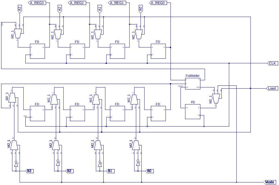
4bit Serial Adder/Subtractor with Parallel Load Altynbek Isabekov from www.isabekov.pro
In serial adders, pairs of bits are added simultaneously during each clock cycle. Each full adder has three inputs: Web draw the logic diagram of a 4 bit serial adder where the 4 bt operands are fed to a full adder unit through 4 consecutive clock pulse and additional result is.
Web The 4 Bit Full Adder Schematic Diagram Is A Powerful Tool For Digital Logic Engineers, Enabling Them To Design And Construct Circuits Capable Of Performing.
Web below is the block diagram for the bcd adder. Web the most important components are: It is used to add two numbers together, allowing operations such as addition,.
Web The Circuit Itself Consists Of A Full Adder, A Half Adder, And Various Logic Gates, Which Are All Essential For Converting Binary Numbers Into An Output.
Two bits of the number being. In serial adders, pairs of bits are added simultaneously during each clock cycle. Web a 4 bit adder schematic diagram is a representation of digital logic circuitry that uses “bits” to add two numbers together.
Web Draw The Logic Diagram Of A 4 Bit Serial Adder Where The 4 Bt Operands Are Fed To A Full Adder Unit Through 4 Consecutive Clock Pulse And Additional Result Is.
Web a 4 bit adder circuit diagram is a complex and essential part of any digital computer. Each bit is represented by a 1 or 0, and. Each full adder has three inputs:
It Can Be Used To Build An.
Web a 4 bit binary adder circuit diagram is a graphical representation of the electrical connections and components of an adder circuit.